2.1. HLS Tasks#
A high-level C/C++ specification of a DSP kernel is untimed. This means that the C/C++ specification describes only the logical operations in a sequential manner. No description is provided about the synchronous timing of the operations in the sequence with respect to any clock. Indeed, if the C/C++ specification were built to run on a CPU, the time it would take to complete an operation as well as the transition time from one operation to the next would both be stochastic in general.
A RTL specification of a DSP kernel is, on the other hand, timed in the sense that all operations in the specification are synchronous to a clock. Thus, it is the job of the HLS tool to construct a timed RTL specification of the DSP kernel from the untimed C/C++ specification. In addition, the HLS tool needs to construct a digital architecture to implement the logical operations described in the C/C++ specification. A typical digital architecture for the DSP kernel includes:
data path
control logic
memory, AXI4, and other interfaces.
The main functionality of the DSP kernel is implemented in the data path, which consists of:
storage elements, e.g., registers and memories,
functional units, e.g., multipliers and arithmetic logic units, and
interconnect elements, e.g., multiplexers, tri-state drivers, buses.
The list below shows the sequence of tasks that the HLS tool needs to perform in order to produce the RTL specification of a DSP kernel from the high-level C/C++ specification:
Compilation: The HLS tool compiles the C/C++ code that specifies the DSP kernel. Code optimizations are also performed to try to meet the design constraints. This step is equivalent to the compilation step in a typical C/C++ compiler, but with perhaps a different set of optimization objectives.
Scheduling: The HLS tool determines which operations should occur in each clock cycle and the amount of PL resources needed to support the operations in that clock cycle.
Binding: The HLS tool assigns specific PL resources to implement each scheduled operation as well as memories and registers required. Resource sharing is also performed so that the same sets of resources can be re-used by operations scheduled to different clock cycles. RTL implementations of the scheduled operations are produced in this step.
Control logic extraction: The HLS tool creates a finite state machine (FSM) that is responsible for sequencing the scheduled operations.
External interface generation: The HLS generates external interfaces for the DSP kernel.
RTL generation: The HLS synthesizes the RTL specification of the complete DSP kernel.
The following two illustrative examples, taken directly from [AMD-Xilinx24c], help to explain the HLS tasks listed above.
2.1.1. Scheduling and Binding Example#
Consider the following C/C++ function that specifies a simple DSP kernel:
int ex1(char x, char a, char b, char c) {
  int y;
  y = x*a+b+c;
  return y;
}
where the
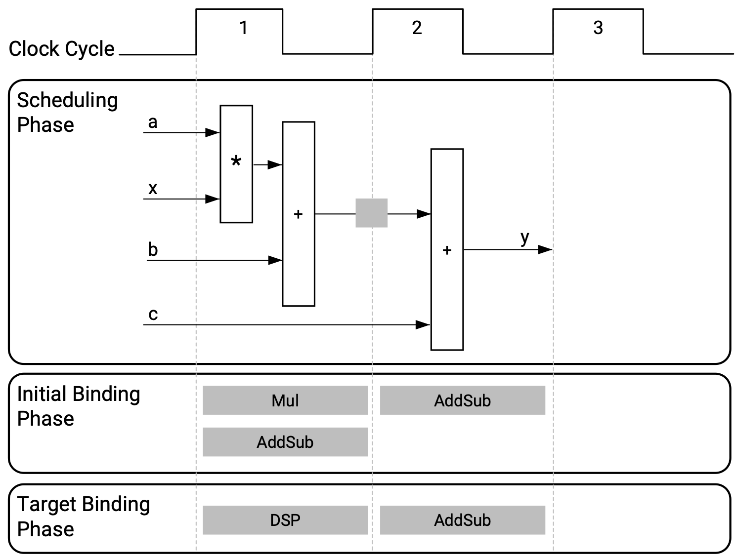
charvariablexandintvariableyrespectively are the input and output of the kernel and thecharvariablesa,b, andcare kernel parameters.The figure below shows the assignments produced by the HLS tool in the scheduling and binding tasks:

Fig. 2.1 Example showing the assigments in the HLS scheduling and binding tasks (image taken from [AMD-Xilinx24c])#
In the scheduling task, the HLS tool determines the function
ex1can be implemented in two clock cycles:The multiplication and first addition
x*a+bare scheduled to clock cycle 1.The result of the operation in clock cycle 1 is to be stored in a register.
The second addition
+cis scheduled to clock cycle 2.
The binding task is performed in two phases:
In the initial binding phase, the HLS tool assigns a combinational multiplier (
Mul) to the multiplication operation and a combinational adder/subtractor (AddSub) to each of the two additions.In the target binding phase, the HLS tool decides to use a DSP slice, in lieu of the
MulandAddSub, to implement the multiplication and addition together in clock cycle 1.
2.1.2. Control Logic Extraction Example#
Consider the following C/C++ function that specifies another simple DSP kernel:
 void ex2(int in[3], char a, char b, char c, int out[3]) {
   int x, y;
   for (int i = 0; i < 3; i++) {
     x = in[i];
     y = a*x+b+c;
     out[i] = y;
   }
}
whose functionality is the same as the kernel in Section 2.1.1 except that both the input and output of the kernel are \(3\)-element
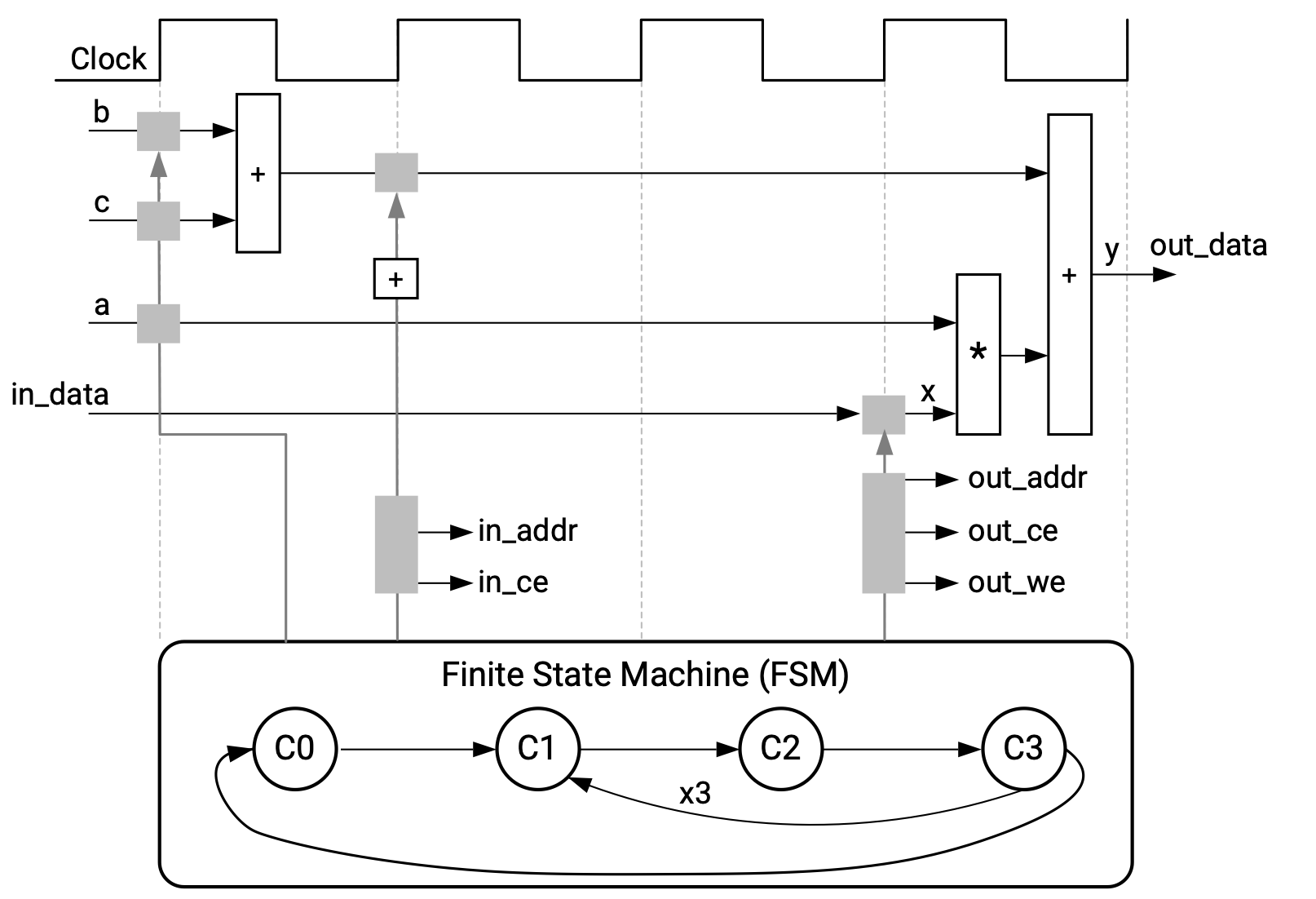
intarrays.The figure below shows the FSM generated by the HLS tool in the control logic extraction task to sequence the scheduled operations and the I/O port assignment produced in the interface generation task: assignments produced by the HLS tool in the scheduling and binding tasks:

Fig. 2.2 Example showing the FSM and I/O ports generated in the control logic extraction task (image taken from [AMD-Xilinx24c])#
In the compilation and scheduling tasks, the HLS tool constructs a schedule that is different than the one for the function
ex1in Section 2.1.1 because the current schedule is more efficient for the for-loop inex2(no need to recalculateb+cin each iteration).In the binding task, the input and output arrays
inandoutare bound to the block RAM resource in the PL. The HLS tool automatically creates data ports, address ports, and any required chip-enable or write-enable signals to access the block RAM. The other variables are bound to registers. Each of the parameter input variablesa,b, andcis mapped to an input 8-bit data port.In the control logic extraction task, control logics for accessing the RAM and the input data ports for the parameters, such as data ports, address ports, chip-enable (ce) and write-enable (we) signals are created. The HLS tool also construct the FSM as shown in Fig. 2.2 to sequence the operation schedule stepping through the state transition sequence shown below from one clock cycle to the next:
\[\begin{equation*} C_0 \rightarrow C_1 \rightarrow C_2 \rightarrow C_3 \rightarrow C_1 \rightarrow C_2 \rightarrow C_3 \rightarrow C_1 \rightarrow C_2 \rightarrow C_3 \ (\rightarrow C_0 \rightarrow C_1 \rightarrow \cdots \,) \end{equation*}\]to implement the for-loop in the function
ex2. The FSM controls the timing of RAM address and control signal generation to read from and write to the RAM as well as the timing of reading from the input ports and internal registers and writing to the internal registers. For example, the address toin[0]is generated in the clock cycle when the FSM first enters the state \(C_1\) so that the RAM content at that address is read into the internal registerxin the clock cycle when the FSM first enters \(C_2\), and the address toout[0]is generated at the same clock cycle so that the calculation result in the clock cycle when the FSM first enters \(C_3\) can be stored.If the function
ex2is a top-level HLS function in a VAAD flow, theintvectorsinandoutwill be mapped to global memory resources, and the operation schedule generated in the scheduling and binding tasks will be different. The global memory and scalar ports will be accessed through the AXI4-M and AXI4-Lite protocols in the VAAD flow. Kernel control will also be supported through the AXI4-Lite protocol. In that case, AXI4-M and AXI4-Lite interfaces will be generated by the HLS tool in the external interface generation task. All these will be further discussed in Section 5.
